

VLSI Design Articles
Top 8 Critical Challenges Faced by VLSI Designers in 2025
Future Scope of VLSI Design: Things You Must Know
30 VLSI Interview Questions and Answers for Professionals
Types of VLSI Design: A Practical Guide for Beginners (2025)

Get In Touch For Details! Request More Information

The semiconductor industry will reach $1 trillion by 2030, creating VLSI design jobs worldwide. VLSI design careers promise great growth potential with starting salaries of ₹5.8 LPA for newcomers that can reach ₹25.3 LPA for seasoned professionals.
Government programs like India’s semiconductor mission have created a welcoming environment for future VLSI professionals. But it can be very confusing to navigate this industry without any prior knowledge, and this is where we’ll be helping you out so that you can build a successful career in VLSI Design.
Hence in this article, we’ll take a closer look at the top 8 VLSI design job roles you can pursue. You’ll learn about their responsibilities and skills needed to excel in each role. Fresh graduates and career switchers will see how these positions help create integrated circuits that drive modern technology.
Table of contents
- What is VLSI Design?
- Top 8 VLSI Design Job Roles
- 1) ASIC Design Engineer
- 2) FPGA Design Engineer
- 3) VLSI Design Verification Engineer
- 5) DFT (Design for Test) Engineer
- 6) Analog/Mixed-Signal Design Engineer
- 7) Semiconductor Process Engineer
- 8) Embedded Systems Engineer
- Concluding Thoughts…
- FAQs
- Q1. What are the key responsibilities of a VLSI Design Engineer?
- Q2. What skills are essential for a career in VLSI design?
- Q3. How does the role of a Physical Design Engineer differ from other VLSI positions?
- Q4. What is the significance of Design for Test (DFT) in VLSI?
- Q5. How are emerging technologies impacting VLSI design careers?
What is VLSI Design?
VLSI design is a revolutionary process that puts millions or billions of transistors on a single silicon chip. The technology emerged in the 1970s and altered the map of semiconductor and communication technologies.
VLSI design works through an iterative approach that transforms an original concept into a manufacturable device across five design abstraction levels. These levels include functional architecture, register transfer level, logic design, circuit design, and physical design. Each level plays a vital role in creating complex integrated circuits.
The power of VLSI design comes from its ability to handle design complexity through hierarchy and abstraction. Designers can work with functional blocks built from cells that are made from transistors by breaking down large systems into manageable units. CMOS has remained the technology of choice since the early 1980s.
Top 8 VLSI Design Job Roles
VLSI professionals can build rewarding careers in the semiconductor industry. Each position needs specific skills and plays a unique role in developing chips.
The VLSI job market thrives in many industries. You’ll find opportunities in semiconductor manufacturing, telecommunications, aerospace, defense, and biomedical sectors. These roles need experts who can design and optimize integrated circuits while maintaining high performance and manufacturability.
Let’s look at the most popular VLSI design roles:
1) ASIC Design Engineer
ASIC Design Engineers are the life-blood of VLSI design. They create custom integrated circuits for specific applications and are responsible for designing and developing custom semiconductor chips tailored for specific applications such as AI processors, networking devices, and high-performance computing.
These professionals handle complex SOC design responsibilities. Their main duties include writing microarchitecture specifications and implementing intricate logic designs.
Skills Needed:
- Hardware Description Languages (HDLs): Proficiency in Verilog, VHDL, and SystemVerilog for RTL design and verification.
- EDA Tools: Experience with Cadence, Synopsys, and Mentor Graphics for ASIC design, synthesis, and timing analysis.
- Low-Power Design: Techniques such as clock gating, power gating, and multi-Vt optimization.
- DFT (Design for Testability): Knowledge of scan chains, ATPG, and BIST methodologies.
- Backend Design Awareness: Exposure to floorplanning, placement, routing, and signoff verification.
Career Progression:
- Entry-Level: ASIC Design Engineer
- Mid-Level: Senior ASIC Design Engineer
- Advanced: ASIC Lead/Staff Engineer → Principal Engineer → ASIC Design Manager
- Leadership Roles: Director of VLSI/Chip Design → VP of Engineering → CTO
Salary in India:
- Entry-Level (0-3 years): ₹7-15 LPA
- Mid-Level (3-8 years): ₹15-30 LPA
- Senior-Level (8+ years): ₹30-60 LPA
2) FPGA Design Engineer
FPGA Design Engineers play a vital role in the VLSI industry. They create customizable hardware solutions that can be reprogrammed after manufacturing. These engineers specialize in designing, implementing, and testing digital circuits using FPGA technology.
They work on RTL (Register Transfer Level) design, verification, and optimization to develop high-performance, low-power, and reconfigurable hardware solutions. These skilled professionals blend technical expertise with creative problem-solving to develop flexible circuit designs.
Skills needed:
- Proficiency in VHDL, Verilog, and SystemVerilog for RTL design
- Strong understanding of digital design principles, timing analysis, and FPGA architectures
- Experience with FPGA design tools like Xilinx Vivado, Intel Quartus, and Lattice Diamond
- Knowledge of high-speed interfaces (PCIe, DDR, Ethernet) and embedded systems
- Expertise in synthesis, place-and-route, and power optimization
- Debugging and verification using simulation tools and hardware debugging techniques
Career Progression:
- Entry-Level: FPGA Design Engineer / RTL Design Engineer
- Mid-Level: Senior FPGA Engineer / FPGA Verification Engineer
- Advanced-Level: FPGA Architect / Principal FPGA Engineer
- Leadership Roles: FPGA Team Lead / Hardware Engineering Manager
Salary in India:
- Entry-Level (0-3 years): ₹6-12 LPA
- Mid-Level (4-8 years): ₹12-25 LPA
- Senior-Level (8+ years): ₹25-50 LPA

3) VLSI Design Verification Engineer
VLSI Design Verification leads the way in semiconductor reliability testing. These experts make sure integrated circuit designs work perfectly before manufacturing starts, which saves both money and time.
Their main job is to check if designs match the given specifications. A systematic approach helps engineers find and fix design problems early.
Skills needed:
- Proficiency in SystemVerilog, UVM, and Verilog for testbench development
- Experience with simulation tools like Cadence Xcelium, Synopsys VCS, and Mentor Questa
- Strong knowledge of functional verification, assertion-based verification, and formal verification
- Understanding of RTL design, FPGA prototyping, and debugging techniques
- Expertise in scripting languages (Python, Perl, or Tcl) for automation
Career Progression:
- Entry-level: Verification Engineer (0–3 years)
- Mid-level: Senior Verification Engineer (3–7 years)
- Advanced: Verification Lead / Principal Engineer (7–12 years)
- Expert: Verification Architect / Verification Manager (12+ years)
Salary in India:
- Entry-level: ₹6-12 LPA
- Mid-level: ₹12-25 LPA
- Senior-level: ₹25-50 LPA
4) Physical Design Engineer
Physical Design Engineers connect logical circuit descriptions with manufacturable silicon layouts. These professionals change abstract hardware logic into real configurations of physical gates and interconnecting wires. Their expertise helps create final silicon products that meet design specifications and maintain high yield rates.
Skills needed:
- Expertise in RTL-to-GDSII flow, including synthesis, place & route, and physical verification
- Proficiency in tools like Cadence Innovus, Synopsys IC Compiler, and Mentor Calibre
- Strong understanding of timing analysis, power optimization, and signal integrity
- Knowledge of process nodes (e.g., 7nm, 5nm, 3nm) and semiconductor fabrication processes
- Scripting skills in Python, TCL, or Perl for automation
Career Progression:
- Entry-level: Physical Design Engineer
- Mid-level: Senior Physical Design Engineer
- Advanced: Physical Design Lead / Staff Engineer
- Expert: Physical Design Manager / Principal Engineer / VLSI Architect
Salary in India:
- Entry-level: ₹6-12 LPA
- Mid-level: ₹15-25 LPA
- Senior-level: ₹30-50 LPA+
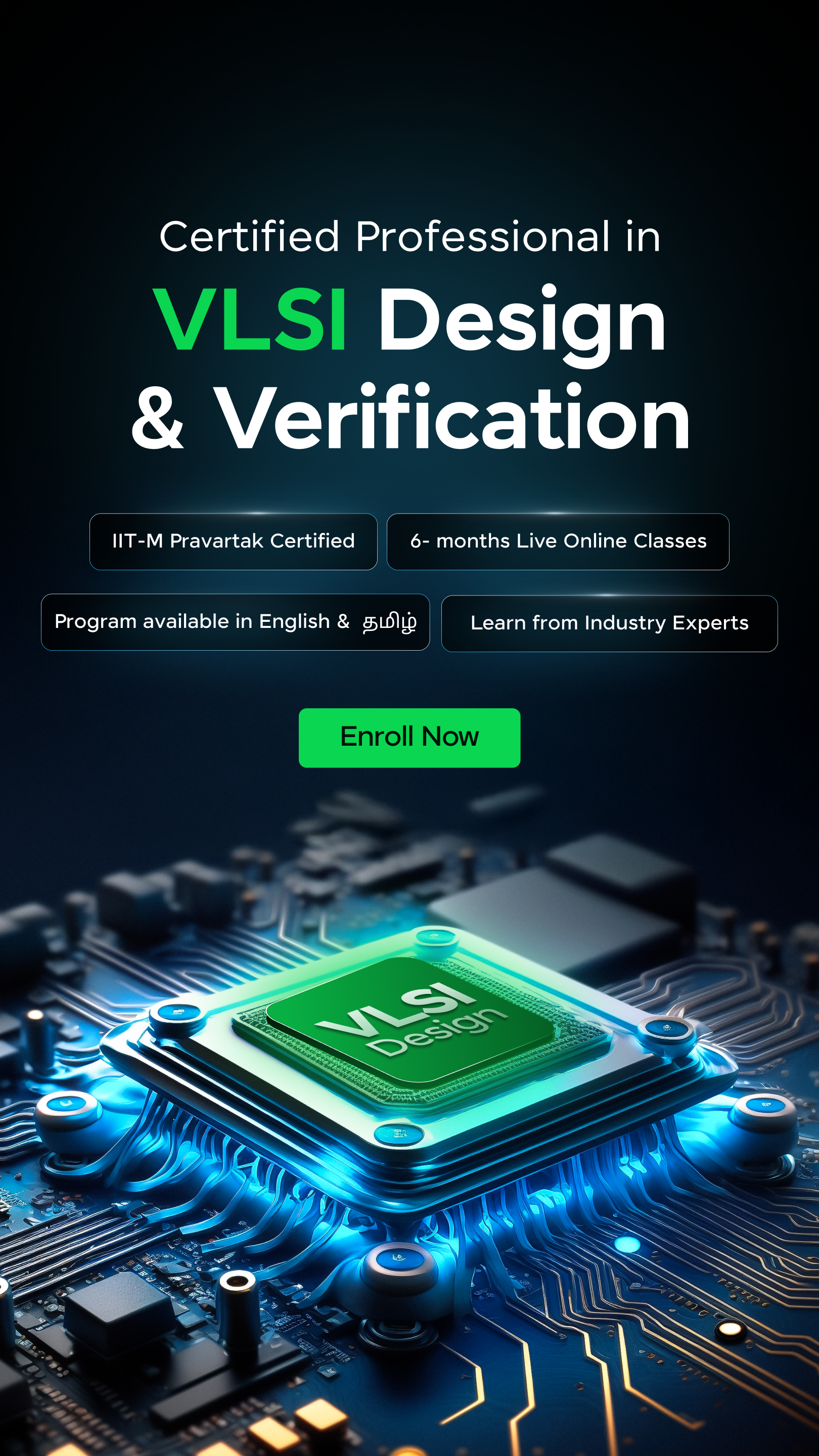
To kickstart your career in VLSI Design, the GUVI VLSI Design & Verification Course offers hands-on training in RTL design, FPGA programming, ASIC verification, and industry-standard EDA tools. Designed by IIT Madras-certified experts, this course provides job-ready skills to help you land top VLSI roles in chip design, embedded systems, and semiconductor industries.
5) DFT (Design for Test) Engineer
DFT Engineers are vital in ensuring integrated circuits’ quality and reliability through advanced testing methods. These professionals build specialized test features right into chip designs. This approach enables quick fault detection and diagnosis during manufacturing.
DFT Engineers keep their focus on three vital performance metrics: speed, budget-friendly solutions, and repeatable testing procedures. Their expertise covers many areas, from scan-based testing to built-in self-test (BIST) capabilities.
Skills needed:
- Strong knowledge of DFT methodologies (Scan, BIST, ATPG, JTAG)
- Proficiency in hardware description languages (Verilog, SystemVerilog, VHDL)
- Hands-on experience with EDA tools (Synopsys DFT Compiler, Cadence Modus, Tessent)
- Understanding of fault modeling and test coverage analysis
- Expertise in timing analysis, logic synthesis, and debugging
- Familiarity with scripting languages (TCL, Perl, Python) for automation
Career Progression:
- Entry-Level: DFT Engineer / Test Engineer
- Mid-Level: Senior DFT Engineer / Lead DFT Engineer
- Senior-Level: DFT Architect / Principal DFT Engineer
- Executive-Level: DFT Manager / Director of Test Engineering
Salary in India:
- Entry-Level (0-2 years): ₹8-12 LPA
- Mid-Level (3-7 years): ₹15-25 LPA
- Senior-Level (8+ years): ₹30-50 LPA
6) Analog/Mixed-Signal Design Engineer
Analog/Mixed-Signal Design Engineers face complex challenges in today’s fast-evolving semiconductor world. These specialists excel at integrating both analog and digital components on a single chip. They build sophisticated circuits that process continuous signals alongside discrete digital data, which makes them vital to modern electronics development.
Skills needed:
- Strong foundation in analog circuit design (op-amps, filters, oscillators)
- Proficiency in SPICE simulations and EDA tools like Cadence Virtuoso
- Knowledge of mixed-signal verification techniques (Verilog-AMS, SystemVerilog)
- Understanding of process variations, noise analysis, and layout techniques
- Experience with low-power and high-speed circuit design
Career Progression:
- Entry-Level: Analog Design Engineer / Mixed-Signal Engineer
- Mid-Level: Senior AMS Design Engineer / Lead Circuit Designer
- Advanced-Level: AMS Architect / Principal Engineer / Analog IC Design Manager
- Expert-Level: Fellow / Chief Scientist in AMS Circuit Design
Salary in India:
- Entry-Level: ₹8-12 LPA
- Mid-Level: ₹15-25 LPA
- Senior-Level: ₹30-50 LPA
- Top-Level (Architect/Manager): ₹50+ LPA
7) Semiconductor Process Engineer
Process Engineers direct the complex steps that transform raw silicon into sophisticated integrated circuits in semiconductor manufacturing. They are responsible for developing, optimizing, and maintaining the fabrication processes used in semiconductor manufacturing.
Their expertise brings substantial rewards, with average salaries going beyond six figures. These professionals must excel in multiple areas from photolithography to ion implantation to ensure optimal yield and efficiency in chip production.
Skills needed
- Strong understanding of semiconductor physics and fabrication techniques
- Experience with cleanroom protocols and process control
- Proficiency in using process simulation tools (e.g., TCAD, COMSOL)
- Knowledge of materials science and chemical processes
- Data analysis and problem-solving skills
- Familiarity with semiconductor manufacturing standards and quality control
Career Progression:
- Entry-level: Process Development Engineer
- Mid-level: Senior Process Engineer
- Advanced-level: Process Integration Engineer
- Expert-level: Fabrication Manager / R&D Director
Salary in India:
- Entry-level: ₹6–10 LPA
- Mid-level: ₹12–20 LPA
- Senior-level: ₹25+ LPA
8) Embedded Systems Engineer
Embedded Systems Engineers blend hardware and software expertise to build specialized computing solutions that fit into larger electronic systems. They design, develop, and optimize hardware-software systems for real-time applications.
They work with microcontrollers, processors, and embedded operating systems to build efficient, low-power, and high-performance embedded solutions. Their role includes firmware development, system debugging, and integrating hardware components with software for applications like automotive electronics, IoT devices, and medical equipment.
Skills needed:
- Proficiency in C, C++, Python, and assembly language
- Experience with microcontrollers (ARM, PIC, AVR) and FPGA programming
- Knowledge of RTOS, Linux kernel, and device drivers
- Hardware debugging using oscilloscopes, logic analyzers
- Understanding of communication protocols (UART, SPI, I2C, CAN)
- Power optimization and real-time performance tuning
Career Progression:
- Entry-level: Embedded Systems Engineer, Firmware Engineer
- Mid-level: Senior Embedded Engineer, Embedded Software Architect
- Advanced-level: Embedded Systems Lead, SoC Architect, IoT Solutions Architect
- Expert-level: Embedded Systems Manager, Technical Director, CTO (Embedded Solutions)
Salary in India:
- Entry-level (0-3 years): ₹5-8 LPA
- Mid-level (4-7 years): ₹10-18 LPA
- Senior-level (8+ years): ₹20-35 LPA
Concluding Thoughts…
VLSI design careers are packed with exceptional opportunities in various specializations. Each position just needs specific technical expertise.
Technical mastery and strong collaboration skills are essential to thrive in VLSI design. VLSI professionals must adapt to emerging technologies like AI and quantum computing to stay competitive in this ever-changing field.
The semiconductor industry will reach $1 trillion by 2030, which will give a steady stream of opportunities for skilled VLSI designers. A clear understanding of these roles will help you choose the right career path and develop the skills to excel in semiconductor design and development.
FAQs
A VLSI Design Engineer is responsible for designing and developing high-performance, low-power integrated circuits. They create RTL designs using hardware description languages, perform simulations, troubleshoot issues, and optimize circuits for specific applications.
Essential skills for VLSI design include proficiency in hardware description languages (like Verilog or VHDL), knowledge of digital circuit design, familiarity with EDA tools, understanding of semiconductor physics, and strong problem-solving abilities. Expertise in specific areas like analog design or verification may be required for certain roles.
A Physical Design Engineer focuses on transforming logical designs into physical layouts. They handle tasks such as floorplanning, placement, clock tree synthesis, and routing. This role requires expertise in physical design tools and techniques to optimize chip area, power consumption, and timing.
Design for Test is crucial in VLSI as it enables efficient fault detection and diagnosis throughout the manufacturing process. DFT Engineers incorporate test features into chip designs, develop test infrastructures, and work on optimizing test quality and time. This helps reduce design iterations and accelerate time-to-market for semiconductor products.
Emerging technologies like artificial intelligence, machine learning, and quantum computing are creating new specializations within VLSI design. These advancements are driving demand for professionals who can innovate in areas such as ultra-low power designs, advanced packaging techniques, and AI-driven design methodologies. Continuous learning is essential to stay competitive in this evolving field.
Career transition

About the Author
Jaishree Tomar
A recent CS Graduate with a quirk for writing and coding, a Data Science and Machine Learning enthusiast trying to pave my own way with tech. I have worked as a freelancer with a UK-based Digital Marketing firm writing various tech blogs, articles, and code snippets. Now, working as a Technical Writer at GUVI writing to my heart’s content!
Connect with me @


 5")


Did you enjoy this article?