
Latest VLSI Design Trends 2025: Essential Updates for Designers
Jan 31, 2025 6 Min Read 3039 Views
(Last Updated)
The semiconductor industry faces a defining moment. Chip designs grow more intricate and resource-intensive each day. VLSI designers must be proactive about evolving technologies and methodologies that will shape tomorrow’s integrated circuits.
Modern electronic systems have reached unprecedented levels of sophistication. This evolution brings fresh challenges and opportunities to VLSI design. AI-powered automation and cutting-edge manufacturing processes have altered the map of chip design.
This article outlines the top VLSI design trends that will define 2025. You’ll discover everything about next-generation design tools, security-first approaches, and power optimization strategies.
Table of contents
- What is VLSI Design?
- Top VLSI Design Trends in 2025
- 1) Next-Generation AI-Driven Design Automation
- 2) Advanced Manufacturing Technologies
- 3) Power Optimization Strategies
- 4) Security-First Design Approaches
- 5) Future-Ready Design Tools
- Takeaways…
- FAQs
- Q1. What are the key VLSI design trends in 2025?
- Q2. How is artificial intelligence impacting VLSI design?
- Q3. What advancements are being made in power optimization for VLSI designs?
- Q4. How are security concerns being addressed in modern VLSI design?
- Q5. What role do cloud-based platforms play in VLSI design?
What is VLSI Design?
VLSI (Very Large Scale Integration) emerged in the 1970s as a process to combine billions of transistors onto a single chip. VLSI design forms the backbone of modern electronic systems. It enables the creation of complex integrated circuits that power our digital world.

VLSI design combines multiple components into a unified system. A typical VLSI chip integrates several elements:
- Central Processing Unit (CPU)
- Read-Only Memory (ROM)
- Random Access Memory (RAM)
- Additional logic components
VLSI design requires a deep understanding of technical aspects like timing constraints, power management, and circuit testing. Engineers must become skilled at concepts such as setup and hold time, propagation delays, and contamination delays in sequential circuits. Their role includes estimating CMOS circuit characteristics, noise margins, DC response, and RC delay models.
The VLSI design process has evolved substantially since its early days. Engineers now use advanced design automation tools and automated logic synthesis to manage billions of transistors effectively. This automation creates increasingly complex systems while maintaining reliability.
Top VLSI Design Trends in 2025
The field of Very Large-Scale Integration (VLSI) design is rapidly evolving, driven by the demands of AI, IoT, and high-performance computing.
Key trends include the adoption of advanced node technologies, chiplet-based architectures, and innovations in low-power and 3D IC design. These developments are reshaping the industry, enabling more efficient and scalable semiconductor solutions.
1) Next-Generation AI-Driven Design Automation
AI is revolutionizing chip design. You’ll find AI-driven automation has become crucial to your VLSI design workflow. Machine learning algorithms now handle multidimensional and multivariate data at incredible speeds. Hence, this is one of the top vlsi design trends. Let’s explore these trends in detail:

Machine Learning for Layout Optimization
Machine Learning for Layout Optimization involves using machine learning (ML) techniques to optimize VLSI layouts for performance, area, and power. ML algorithms analyze large datasets of design rules, constraints, and previous layouts to predict optimal placements and routing paths.
These models enable faster convergence on complex designs by automating iterative tasks like floorplanning and congestion analysis. Advanced methods, such as reinforcement learning, enhance optimization by learning from design feedback.
This approach not only reduces time-to-market but also ensures superior design efficiency and reliability in next-generation VLSI systems.
Automated Verification Systems
Automated verification systems, powered by AI, are transforming VLSI design by enhancing accuracy and reducing verification cycles. These systems leverage machine learning algorithms to identify design flaws, optimize test coverage, and predict potential issues early in the design flow. By automating tasks like functional verification, timing analysis, and power optimization, they significantly reduce human intervention and design turnaround time.
Advanced AI-driven solutions also enable adaptive learning, continuously improving verification efficiency as designs grow in complexity. This trend ensures faster time-to-market and higher reliability in cutting-edge semiconductor designs.
AI-Powered Design Space Exploration
AI-powered design space exploration has changed optimization challenges completely. Synopsys DSO.ai uses reinforcement learning to boost power, performance, and area all at once. This tool gives you:
| Optimization Aspect | Benefit |
| Design Time | Less manual work |
| Quality | Better results through smart learning |
| Efficiency | Quicker path to optimal solutions |
These AI systems keep learning and getting better at predictions. Predictive analytics helps you spot design flaws and bottlenecks early. This creates faster design cycles and improved outcomes.
AI-driven tools explore different floorplan options by testing various aspect ratios and placement styles. You can achieve the best results while meeting design constraints and performance targets making it one of the most intuitive vlsi design trends.
2) Advanced Manufacturing Technologies
Manufacturing advances are reshaping VLSI design with breakthrough developments in process nodes and materials. These significant changes will affect design decisions in the coming years. Let’s take a look at all the new changes and discuss about these revolutionary vlsi design trends at length:
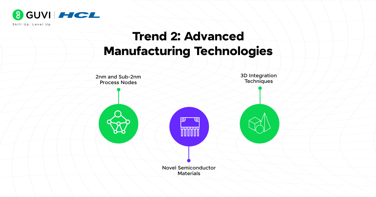
2nm and Sub-2nm Process Nodes
The 2nm and sub-2nm process nodes represent the cutting edge of semiconductor manufacturing, enabling the production of smaller, more efficient transistors. These advanced nodes utilize nanosheet and gate-all-around (GAA) transistor architectures to enhance power efficiency, performance, and density.
They enable chip designers to pack billions of transistors on a single chip, reducing power consumption while improving computational speed. Applications of these technologies span AI, 5G, and high-performance computing, meeting the growing demand for powerful yet energy-efficient devices.
However, challenges like increased manufacturing costs, quantum effects, and defect densities pose significant hurdles to scaling further.
Novel Semiconductor Materials
The adoption of novel semiconductor materials is revolutionizing VLSI design, enabling faster, smaller, and more energy-efficient chips. Materials like Gallium Nitride (GaN) and Silicon Carbide (SiC) offer superior thermal conductivity and higher breakdown voltages, making them ideal for high-performance and power-sensitive applications.
Additionally, 2D materials like graphene and transition metal dichalcogenides (TMDs) are being explored for their exceptional electrical properties, paving the way for next-generation transistors.
These advancements address the limitations of traditional silicon, driving innovation in areas like 5G networks, automotive electronics, and IoT devices, while supporting the industry’s push toward sub-3nm process nodes.
3D Integration Techniques
VLSI design options now extend into the vertical dimension through advanced 3D integration. This technology stacks multiple layers of active devices while managing thermal aspects. This is a big step in the vlsi design trends.
3D integration brings substantial benefits to designs. The implementation challenges need careful planning. Higher transistor density becomes achievable with dense, high-speed interfaces.
These techniques use Through-Silicon Vias (TSVs) and advanced bonding methods to interconnect layers, enabling faster data transfer and reduced power consumption. By minimizing interconnect delays and increasing integration density, 3D integration addresses the challenges of scaling in traditional 2D designs.
Would you like to master VLSI Design and become a pro at designing chips? GUVI’s VLSI Design and Verification Course will be the perfect resource for you with its hands-on learning in digital design, verification, RTL coding, and simulation using industry-standard tools like Verilog and SystemVerilog.
Taught by experienced mentors, it equips you with real-world skills to excel in the semiconductor industry. With live projects, job assistance, and a structured curriculum, this course is your gateway to mastering VLSI Design.
3) Power Optimization Strategies
Power optimization has become crucial in VLSI design. Devices keep getting smaller but need better performance. Design decisions must balance power efficiency and functionality more carefully now than ever. We will now explore these evolving strategies and what makes them one of the top vlsi design trends at length:

Dynamic Power Management Systems
Dynamic Power Management (DPM) systems are an integral part of power optimization strategies in VLSI design. These systems dynamically adjust the power consumption of a chip based on its workload, operating modes, and environmental conditions. VLSI designs work better with smart power management techniques that control system states.
Techniques such as dynamic voltage and frequency scaling (DVFS), power gating, and adaptive body biasing enable significant energy savings while maintaining performance. By selectively powering down inactive components or reducing their operating voltage, DPM minimizes energy wastage without compromising functionality.
These systems are particularly crucial in battery-powered and high-performance devices, aligning with modern demands for energy-efficient and sustainable chip designs.
Leakage Current Reduction Methods
Leakage current, a significant contributor to static power dissipation in VLSI designs, arises from subthreshold conduction, gate oxide tunneling, and junction leakage. Modern power optimization strategies address this through techniques like multi-threshold CMOS (MTCMOS), which uses high-threshold transistors in non-critical paths to reduce leakage while maintaining performance.
Power gating minimizes leakage by shutting off power to inactive circuit regions using sleep transistors. Dynamic voltage scaling (DVS) and body biasing further help control leakage by adjusting threshold voltages. These methods, combined with advanced materials and design-for-manufacturing (DFM) practices, ensure efficient power management in modern chips.
Energy Harvesting Integration
Energy harvesting is emerging as a transformative strategy in VLSI design, enabling chips to harness ambient energy sources such as solar, thermal, or vibrational energy. This integration minimizes dependency on traditional power supplies, significantly reducing power consumption in low-power devices like IoT sensors and wearables.
Advanced power management units (PMUs) are designed to efficiently capture, convert, and store harvested energy while ensuring stable operation. VLSI trends now focus on creating energy-aware architectures with ultra-low power consumption, enabling sustainable and self-powered systems. This innovation aligns with the growing demand for green technology and energy-efficient designs in modern electronics.
4) Security-First Design Approaches
Securing VLSI designs against cyber threats has become crucial in our interconnected world. New malware variants emerge at an alarming rate of almost one million per day. Your chip designs need strong security measures now more than ever. And learning about these new security measures and how to implement them is a must now making them one of the most important vlsi design trends, so let’s dive in:

Hardware Security Features
As cyber threats grow more sophisticated, hardware security has become a critical aspect of VLSI design. Security-first approaches integrate features like Hardware Root of Trust (HRoT) for secure boot processes, Physical Unclonable Functions (PUFs) for device authentication, and encrypted communication channels to safeguard data.
These designs also include tamper-detection mechanisms to identify unauthorized access and side-channel attack mitigations for secure operations. By embedding security at the hardware level, VLSI designs enhance resilience against vulnerabilities and ensure the integrity of modern electronic systems.
Secure Boot Implementation
Secure boot is a critical feature in modern VLSI designs, ensuring that only authenticated and trusted firmware is executed during device startup. It employs cryptographic techniques such as digital signatures and hardware root of trust to validate the integrity of the bootloader and subsequent software.
By integrating secure boot mechanisms directly into the hardware, designers create tamper-resistant systems that guard against malicious code injection and unauthorized modifications.
This approach is particularly vital for applications in IoT, automotive, and critical infrastructure, where security breaches can have severe consequences. The trend highlights the growing emphasis on hardware-level security in VLSI designs to address emerging cyber threats.
Hardware security threats can demonstrate at different design stages, from specification to layout. A security-first approach should tackle vulnerabilities at each abstraction layer. Physical attacks come in many forms, including microprobing and fault injection techniques.
5) Future-Ready Design Tools
VLSI design tools are evolving faster to keep up with complex chip designs. Your toolkit now goes beyond desktop applications and includes cloud-computing and collaborative platforms. The kind of evolution VLSI has seen over the recent years has been pretty phenomenal, and to be on top of your game, you must know these top vlsi design trends:
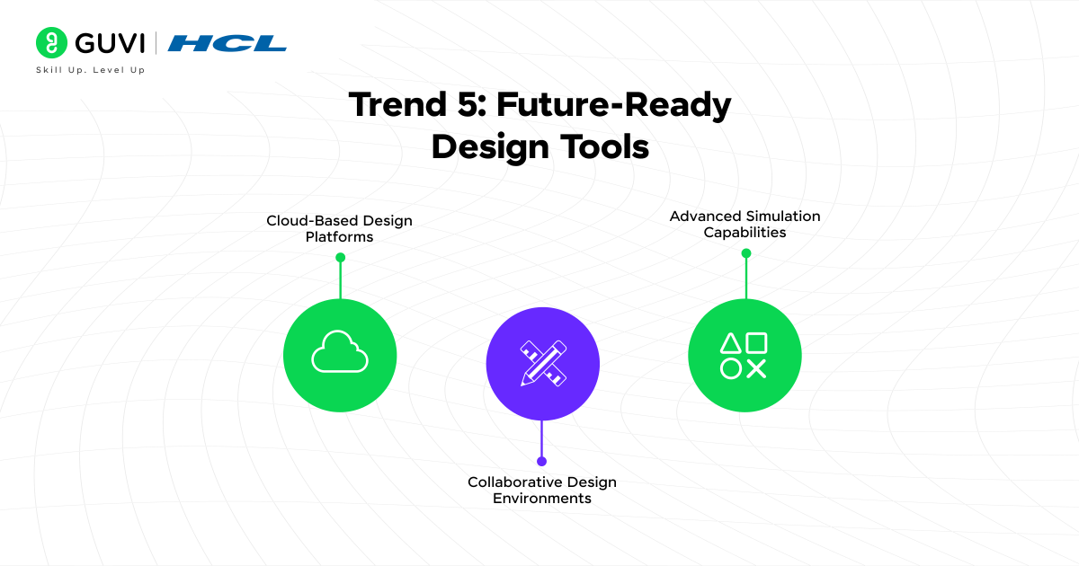
Cloud-Based Design Platforms
Cloud-based design platforms in VLSI provide scalable, on-demand computational resources for chip design and verification tasks. These platforms enable teams to perform complex simulations, design synthesis, and verification without investing in expensive local hardware. Key benefits include faster design cycles, global collaboration, and real-time updates, fostering productivity in geographically dispersed teams.
Their pay-as-you-go model optimizes costs, making cutting-edge tools accessible to smaller design firms. With robust security protocols and AI-driven optimizations, cloud platforms are essential for handling modern VLSI designs’ increasing complexity.
Collaborative Design Environments
Collaborative design environments are transforming VLSI workflows by enabling seamless collaboration among geographically dispersed design teams. These platforms integrate cloud-based design tools, real-time data sharing, and version control to streamline the design process.
They facilitate simultaneous access to design files, enabling engineers to debug, analyze, and optimize circuits collaboratively. Advanced features like automated design rule checks and AI-driven suggestions enhance productivity and minimize errors.
By fostering efficient team coordination, these environments are critical for meeting the complexity and time-to-market demands of modern semiconductor designs.
Advanced Simulation Capabilities
Simulation tools now deliver unmatched accuracy and efficiency. These advanced simulation capabilities help you reach verification closure earlier in the design cycle.
Advanced simulation capabilities are pivotal for addressing the increasing complexity of VLSI designs. Future-ready tools leverage AI-driven simulation algorithms to predict and optimize performance under diverse scenarios, reducing verification time.
Furthermore, integrated debugging environments and support for advanced verification methodologies like SystemVerilog and UVM ensure higher coverage and error detection. These innovations empower engineers to design robust, scalable chips that meet evolving market demands.
Takeaways…
VLSI design is reshaping the scene with breakthrough advances in multiple areas. Your path to becoming a successful VLSI designer now depends on knowing how to use AI-powered automation tools that cut design times and deliver better results.
The future of VLSI design needs you to adapt and learn constantly. Keeping up with new technologies, design methods and these top vlsi design trends will help you create better, more efficient, and secure integrated circuits.
Your focus might be AI acceleration, IoT devices, or high-performance computing – these trends will guide your design choices through 2025 and beyond.
FAQs
The major trends include AI-driven design automation, advanced manufacturing technologies like 2nm process nodes, power optimization strategies, security-first design approaches, and cloud-based collaborative design tools.
AI is revolutionizing VLSI design through machine learning for layout optimization, automated verification systems, and AI-powered design space exploration. These technologies are significantly reducing design time and improving overall chip performance.
Power optimization strategies include dynamic power management systems, leakage current reduction methods, and energy harvesting integration. These techniques help designers balance power efficiency with functionality in increasingly complex chips.
Security-first design approaches incorporate hardware security features, quantum-resistant architectures, and secure boot implementation. These measures protect against both current and future cyber threats, including potential quantum computing attacks.
Cloud-based design platforms offer scalability, accessibility, and cost-efficiency for VLSI designers. They provide on-demand computing resources, enable remote collaboration, and offer advanced simulation capabilities to handle the growing complexity of modern chip designs.


![Top 8 VLSI Design Job Roles [2025] 10 vlsi design job roles](https://www.guvi.in/blog/wp-content/uploads/2025/03/Top-8-VLSI-Design-Job-Roles.png)






Super good. All the emerging areas are covered.